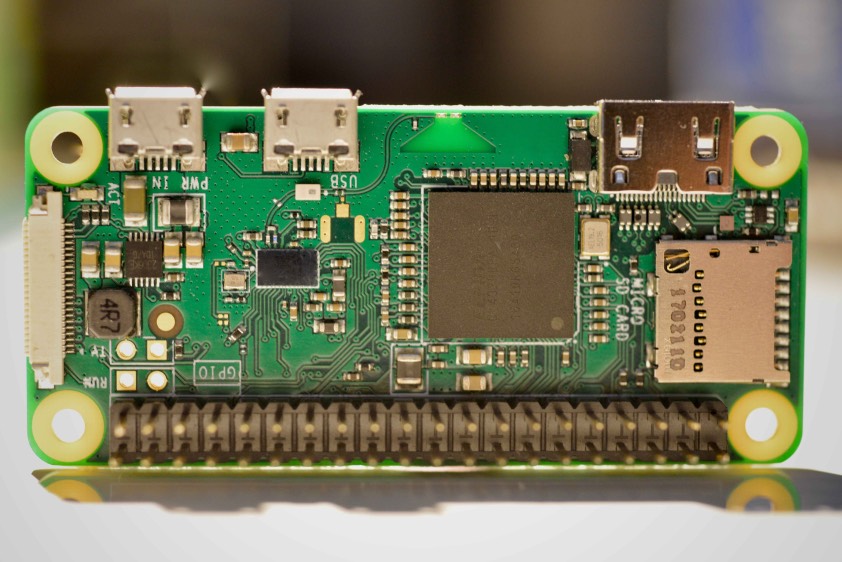
Printed Circuit Boards (PCBs) serve as the foundation for modern electronics, and understanding the materials and technologies involved in their manufacturing process is crucial.
One of the primary materials in PCB production is the substrate, typically composed of fiberglass reinforced with epoxy resin (FR-4). This robust substrate provides mechanical support to the board and serves as an insulating base for the circuitry.
Copper is another essential material, forming the conductive pathways on the PCB. Copper foils are laminated onto the substrate, and the excess copper is removed through etching, leaving behind the desired circuitry pattern.
Advanced technologies play a pivotal role in manufacturing. Surface Mount Technology (SMT) and Through-Hole Technology (THT) are two primary assembly methods. SMT involves placing components directly onto the board's surface, enabling higher component density and automated assembly. THT, on the other hand, involves inserting component leads into pre-drilled holes on the board, providing mechanical strength but with lower component density.
The manufacturing process incorporates various techniques like soldering, where components are affixed to the board. Both lead-free and leaded soldering methods are utilized, with lead-free soldering gaining traction due to environmental and health concerns associated with leaded solder.
Furthermore, technologies like Vias (plated through-holes) and HDI (High-Density Interconnect) allow for increased circuit density, enabling more complex designs in smaller spaces. These advancements have significantly contributed to the miniaturization and enhanced functionality of electronic devices.
Materials and technologies in PCB manufacturing continually evolve to meet the demands of rapidly advancing technologies. Innovations in materials, assembly techniques, and circuit integration methods pave the way for more efficient, compact, and high-performance PCBs that drive the innovation in modern electronics.