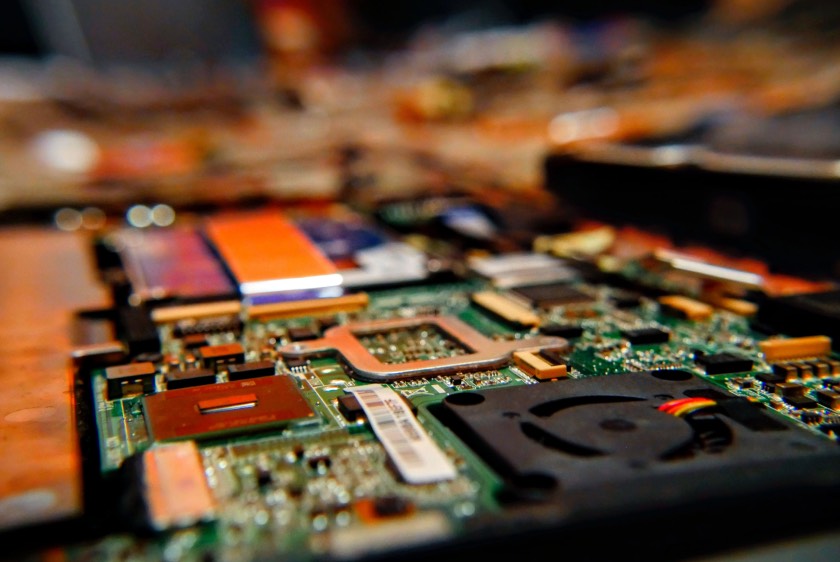
PCBA (Printed Circuit Board Assembly) production involves the process of assembling electronic components onto a printed circuit board (PCB) to create a functional electronic device. Here is a general overview of the PCBA production process:
PCB Fabrication: The first step is to manufacture the PCB itself. This involves designing the PCB layout using specialized software and then sending the design files to a PCB manufacturer. The manufacturer produces the PCB by etching copper layers, drilling holes, applying solder mask and silk screen, and creating the necessary circuitry patterns.
Component Procurement: Once the PCBs are ready, the next step is to procure the required electronic components for assembly. These components can include resistors, capacitors, integrated circuits, connectors, and other active and passive devices. Components can be sourced from various suppliers, and it's important to ensure their quality, compatibility, and availability.
Component Placement: In this stage, the components are placed onto the PCB according to the design specifications. This can be done manually by skilled technicians or using automated equipment like pick-and-place machines. The machines use vision systems to accurately position and place components onto the PCB with high speed and precision.
Soldering: Once the components are placed on the PCB, the next step is soldering to establish electrical connections. There are two main methods of soldering:
a. Wave Soldering: This method is used for through-hole components. The PCB is passed over a wave of molten solder, which forms connections between the component leads and the PCB pads.
b. Reflow Soldering: This method is used for surface-mount components. The PCB is heated in a reflow oven, causing the solder paste previously applied to the PCB pads to melt, creating the connections.
Inspection and Testing: After soldering, the assembled PCBs undergo inspection and testing to ensure quality and functionality. Automated optical inspection (AOI) systems and other testing equipment are used to check for solder defects, component placement accuracy, and electrical connectivity. Functional testing may also be performed to verify the proper operation of the assembled electronic device.
Post-Assembly Processes: Once the inspection and testing are completed, additional processes may be carried out, such as cleaning the PCB to remove any flux residues or contaminants. Conformal coating or encapsulation might also be applied to protect the PCB from environmental factors like moisture or dust.
Packaging and Shipping: Finally, the assembled and tested PCBAs are packaged according to the requirements and specifications of the customer. They are then prepared for shipping or further integration into final products.
It's important to note that PCBA production can vary depending on factors such as the complexity of the PCB design, the volume of production, the specific industry requirements, and the level of automation used in the assembly process.