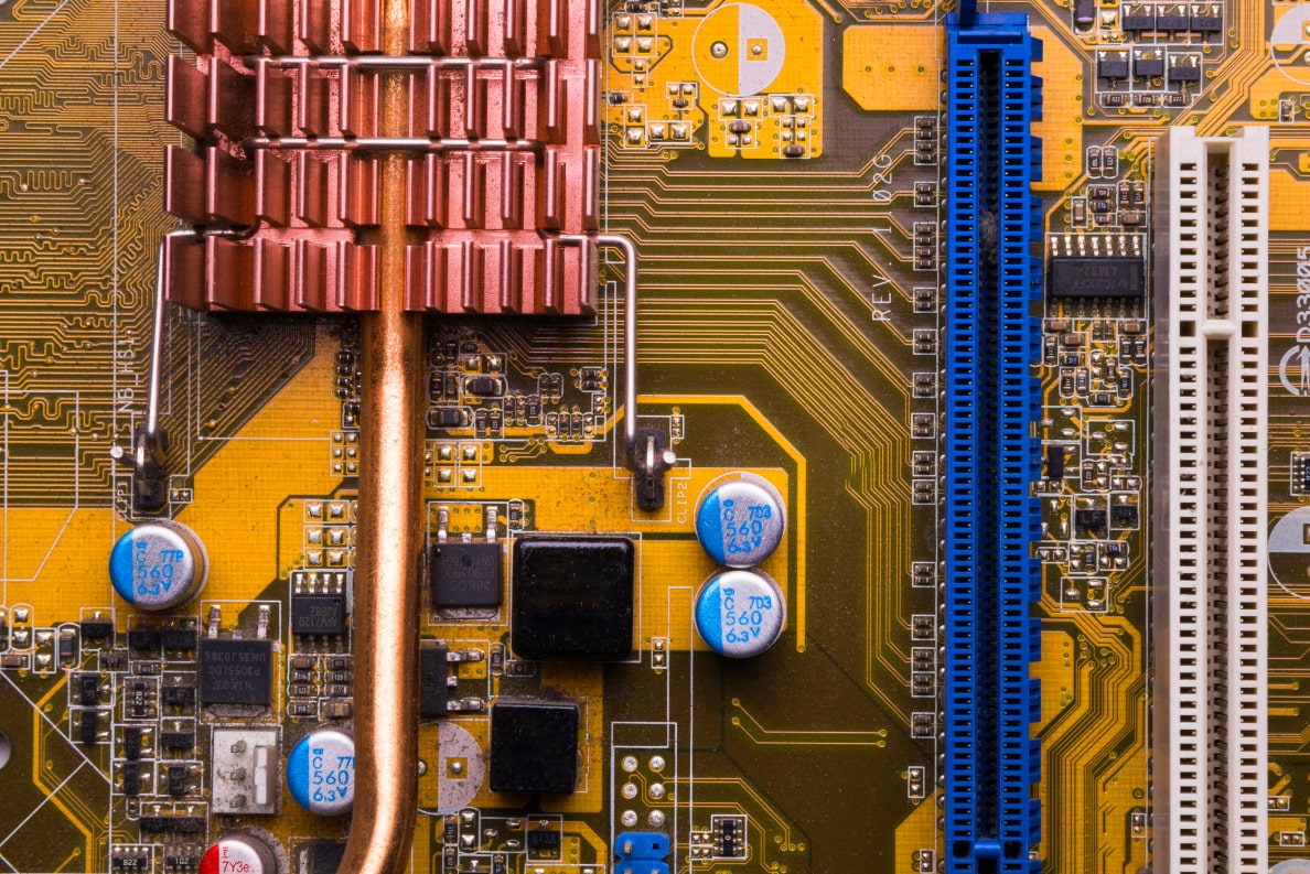
Automatic Optical Inspection (AOI) and testing processes are essential steps in ensuring the quality and reliability of PCB assemblies. AOI systems use cameras and image processing algorithms to inspect PCBs for defects such as missing components, misaligned components, solder joint defects, and solder bridges.
AOI is typically performed after the soldering process to detect and identify any defects that may affect the functionality or reliability of the PCB. By detecting defects early in the manufacturing process, AOI helps prevent costly rework, scrap, and field failures.
In addition to AOI, functional testing and in-circuit testing are commonly used to verify the electrical functionality of PCB assemblies. Functional testing involves subjecting the PCB to simulated operational conditions to ensure that it performs as intended. In-circuit testing, on the other hand, involves testing individual components and circuit nodes to verify proper operation and detect any faults.
Comprehensive testing processes help identify defects and ensure that PCB assemblies meet quality standards and customer requirements. By incorporating AOI, functional testing, and in-circuit testing into the manufacturing workflow, manufacturers can improve product quality, reduce defects, and enhance customer satisfaction.